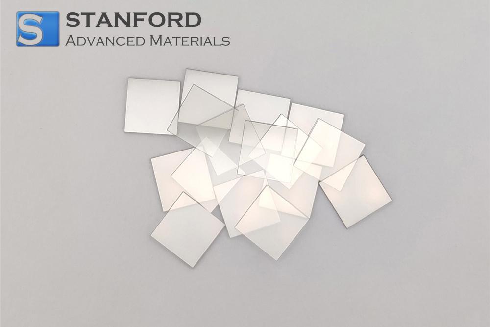
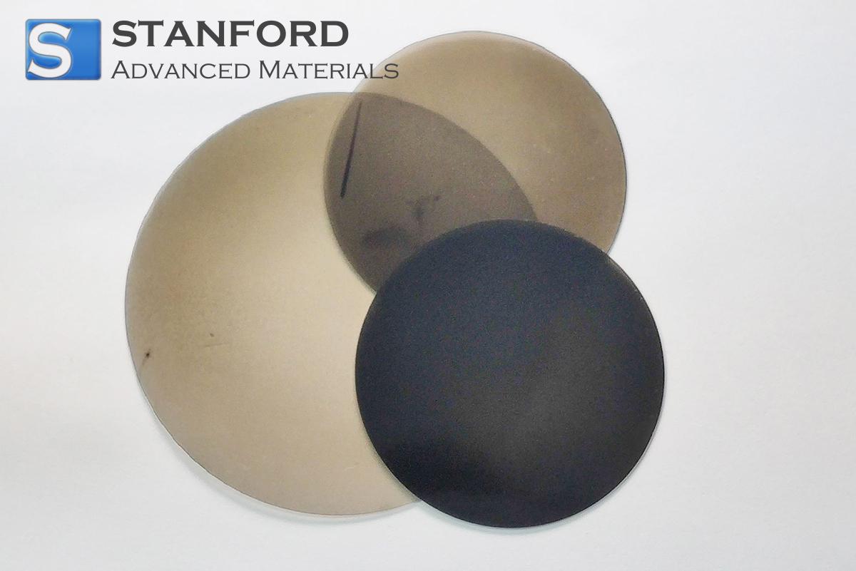
CVD 다이아몬드 웨이퍼 설명
CVD 다이아몬드 웨이퍼는 뛰어난 물리적, 화학적 특성을 가지고 있습니다. 자외선부터 THz까지 거의 연속적인 광학 투명도 대역을 가지고 있습니다. 다이아몬드는 탄소의 한 종류로 높은 내마모성, 화학적 불활성, 우수한 내방사선성으로 경도와 열전도율이 동시에 가장 높습니다. CVD 다이아몬드 웨이퍼는 X-선, 자외선, 적외선, 마이크로파 등 여러 대역 범위에서 사용할 수 있습니다.
높은 에너지 입력, 낮은 유전 손실, 높은 라만 이득, 낮은 빔 왜곡, 내식성 등 일반 광학 재료로 대체할 수 없는 여러 측면에서 중요한 역할을 합니다. CVD 다이아몬드 웨이퍼는 열 전도성이 뛰어나 고열 플럭스 장치에 가장 적합한 열 관리 소재입니다.
CVD 다이아몬드 웨이퍼 사양
|
사양 및 공차
|
|
Grade
|
광학 등급
|
방열판 등급
|
|
유형
|
단결정
|
다결정
|
|
웨이퍼 크기
|
최대 15*15mm² 또는 맞춤형
|
2인치, 3인치, 4인치 또는 맞춤형
|
|
입자 크기
|
-
|
≤10μm
|
|
Dia. 허용 오차
|
﹢0.1, -0mm
|
﹢0.1, -0mm
|
|
두께
|
0.1~2mm
|
0.1~2mm
|
|
두께 허용 오차
|
±0.02mm @ ≤10mm
±0.03mm @10~15mm
|
-
|
|
크리스탈 방향
|
{100}
|
-
|
|
표면 처리
|
광택, Ra<2nm
|
-
|
|
커스터마이징
|
다양한 원소를 이용한 도핑, 표면 연마 및 금속화 서비스
|
|
물리적 특성
|
|
등급
|
광학 등급
|
방열판 등급
|
|
유형
|
단결정
|
다결정
|
|
밀도
|
3.52g/cm³
|
3.51g/cm³
|
|
라만 전체 폭
절반 최대
(FWHM)
|
~2.1cm-¹
|
-
|
|
질소 농도
|
<0.5ppm
|
-
|
|
열 전도성
|
1900~2200 W/(m-K) @ 300K
|
1200~2000 W/(m-K) @ 300K
|
|
투과율
|
>70% @ 1064nm
|
-
|
|
굴절률
|
2.379 @ 10.6μm
|
-
|
|
영의 계수
|
-
|
1000~1100 GPa
|
*자세한 내용은 당사에 문의하시기 바랍니다 .
CVD 다이아몬드 웨이퍼 응용 분야
- 방열판: 다결정 CVD 다이아몬드 웨이퍼는 열전도율이 뛰어나 전력 트랜지스터, 레이저 다이오드 및 기타 반도체와 같은 고전력 전자 기기의 방열판으로 사용됩니다. 방열을 관리하여 중요한 구성 요소의 과열을 방지하는 데 도움이 됩니다.
- 절연 기판: CVD 다이아몬드 웨이퍼는 고성능 반도체의 절연 기판으로 사용됩니다. 전기 절연성과 높은 열전도율 덕분에 전력 장치 및 RF(무선 주파수) 부품에 이상적입니다.
- 광학 창: 단결정 CVD 다이아몬드 웨이퍼는 자외선부터 적외선 범위의 광학적 투명성으로 인해 레이저, 적외선 센서 및 기타 고에너지 광학 시스템을 위한 고성능 광학 윈도우를 만드는 데 사용됩니다.
- 렌즈 및 거울: 다이아몬드는 고출력 레이저 및 군사용 렌즈와 거울과 같이 극한의 내구성과 높은 광 투과율이 요구되는 광학 부품에 사용됩니다.
- 레이저 부품: CVD 다이아몬드는 제조, 의료, 연구 분야에서 사용되는 고출력 레이저 시스템을 비롯하여 극한의 출력 밀도를 성능 저하 없이 견뎌야 하는 레이저 부품에 자주 사용됩니다.
- 의료 기기: 산업용 다이아몬드는 고정밀 수술 도구, 치과용 드릴 등과 같은 일부 의료 분야에서도 사용됩니다. 다이아몬드의 높은 경도와 우수한 내마모성으로 인해 의료 기기의 수명과 정밀도를 향상시킬 수 있습니다.
CVD 다이아몬드 웨이퍼 포장
당사의 CVD 다이아몬드 웨이퍼는 제품의 품질을 원래 상태로 유지하기 위해 보관 및 운송 과정에서 세심하게 취급됩니다.
자주 묻는 질문
Q1. CVD 다이아몬드 웨이퍼의 열 관리 성능은 어떻게 되나요?
CVD 다이아몬드 웨이퍼는 구리를 포함한 대부분의 금속보다 훨씬 높은 열전도율로 인해 열 관리에 탁월합니다. 따라서 고출력 전자제품, 레이저 시스템, LED의 방열판 및 열 확산 애플리케이션에 이상적입니다. 효율적인 열 방출로 과열을 방지하고 디바이스의 안정성과 성능을 향상시킵니다.
Q2. CVD 다이아몬드 웨이퍼는 추가 가공이 가능한가요?
예, 특정 애플리케이션 요구 사항을 충족하기 위해 CVD 다이아몬드 웨이퍼를 추가 가공할 수 있습니다. 일반적인 처리 방법은 다음과 같습니다:
가공: 절단, 연마 및 코팅
도핑: 다른 원소를 추가하여 전기적 특성 수정
표면 처리: 전자 또는 광학 용도에 필요한 표면 마감을 달성하기 위한 에칭 또는 광택 처리
Q3: 다결정 CVD 다이아몬드 웨이퍼와 단결정 CVD 다이아몬드 웨이퍼의 차이점은 무엇인가요?
표를 참조하세요:
|
속성
|
다결정 CVD 다이아몬드 웨이퍼
|
단결정 CVD 다이아몬드 웨이퍼
|
|
구조
|
여러 개의 작은, 무작위 배향 결정
|
단일, 연속 결정 구조
|
|
기계적 특성
|
입자 경계의 영향을 덜 받고 강도가 낮음
|
우수한 경도, 강도 및 내마모성
|
|
열 전도성
|
낮음(입자 경계로 인해)
|
높음, 우수한 열 방출
|
|
광학 특성
|
낮은 선명도, 결함이 있을 수 있음
|
뛰어난 광학적 선명도 및 정밀도
|
|
전기적 특성
|
더 등방성, 덜 제어됨
|
고도로 제어 가능, 방향에 따라 달라짐
|
|
응용 분야
|
산업용 공구, 방열판, 연마재
|
전자, 광학, 고성능 애플리케이션
|
사양
|
Specifications & Tolerances
|
|
Grade
|
Optical Grade
|
Heat Sink Grade
|
|
Type
|
Monocrystal
|
Polycrystal
|
|
Wafer Size
|
Up to 15*15mm², or customized
|
2″, 3″, 4″, or customized
|
|
Grain Size
|
-
|
≤10μm
|
|
Dia. Tolerance
|
﹢0.1, -0mm
|
﹢0.1, -0mm
|
|
Thickness
|
0.1~2mm
|
0.1~2mm
|
|
Thickness Tolerance
|
±0.02mm @ ≤10mm
±0.03mm @10~15mm
|
-
|
|
Crystal Orientation
|
{100}
|
-
|
|
Surface treatment
|
Polished, Ra<2nm
|
-
|
|
Customization
|
Doping with different elements, surface polishing and metallization services
|
|
Physical Properties
|
|
Grade
|
Optical Grade
|
Heat Sink Grade
|
|
Type
|
Monocrystal
|
Polycrystal
|
|
Density
|
3.52g/cm³
|
3.51g/cm³
|
|
Raman Full Width
at Half Maximum
(FWHM)
|
~2.1 cm⁻¹
|
-
|
|
Nitrogen Concentration
|
<0.5 ppm
|
-
|
|
Thermal Conductivity
|
1900~2200 W/(m·K) @ 300K
|
1200~2000 W/(m·K) @ 300K
|
|
Transmittance
|
>70% @ 1064 nm
|
-
|
|
Refractive Index
|
2.379 @ 10.6 μm
|
-
|
|
Young's Modulus
|
-
|
1000~1100 GPa
|
*For detailed information, please contact us.
 바
바
 비즈 & 구체
 볼트 및 너트
 도가니
도가니
 디스크
디스크
 섬유 및 원단
 영화
영화
 플레이크
플레이크
 폼
폼
 호일
호일
 과립
과립
 벌집
벌집
 잉크
잉크
 라미네이트
라미네이트
 덩어리
덩어리
 메시
메시
 메탈라이즈드 필름
 플레이트
플레이트
 파우더
파우더
 Rod
Rod
 시트
시트
 단결정
단결정
 스퍼터링 타겟
 튜브
튜브
 워셔
워셔
 전선
전선
 변환기 및 계산기
 글쓰기
글쓰기


")
")
")
 Crystal")