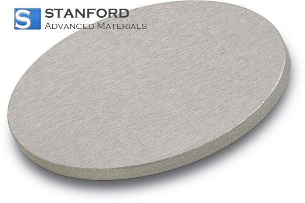
Nickel Silicide (NiSi2) Sputtering Target Description
The Nickel Silicide (NiSi2) Sputtering Target is designed
for advanced deposition techniques in microelectronics and material science
applications. Manufactured with a purity of ≥99%, this target is precisely
engineered to ensure reliable performance in sputtering processes. Its high
melting point of 990℃ coupled with a density of 4.85 g/cm³ makes it an optimal
choice for producing uniform thin films and advanced coatings. Developed by
Stanford Advanced Materials, this product is available in customizable shapes
including standard discs or tailor-made configurations to meet specific
application requirements.
Nickel Silicide (NiSi2) Sputtering Target Applications
· Semiconductor Device Fabrication: Essential for creating
high-quality silicide layers in integrated circuits.
· Surface Engineering: Ideal for depositing conductive and protective coatings.
· Microelectronics: Supports formation of fine features and high-performance
contacts.
· Research and Development: Provides a reliable material for innovative sputtering
and deposition studies.
Nickel Silicide (NiSi2) Sputtering Target Packing
Our Nickel Silicide (NiSi2) Sputtering Target is packaged
with utmost care to maintain its integrity during storage and transport. Custom
packaging options are available, with products typically sealed under
controlled conditions to ensure product purity and performance.
Frequently Asked Questions
Q: What is the primary application of a Nickel Silicide
sputtering target?
A: It is primarily used in semiconductor device fabrication and surface coating
applications, ensuring high-quality film deposition.
Q: How does a purity level of ≥99% benefit this sputtering
target?
A: The high purity minimizes impurities, leading to consistent sputtering
performance and superior quality thin films.
Q: Can the Nickel Silicide sputtering target be customized?
A: Yes, it is available in customized sizes and shapes, including standard
discs or tailor-made configurations.
Q: Which industries commonly use this sputtering target?
A: It is widely used in the semiconductor, microelectronics, and advanced
materials research industries.
Q: How should the product be stored to maintain its quality?
A: It should be stored under controlled conditions, preferably in vacuum-sealed
packaging, to protect it from contamination and maintain its performance.
 바
바
 비즈 & 구체
 볼트 및 너트
 도가니
도가니
 디스크
디스크
 섬유 및 원단
 영화
영화
 플레이크
플레이크
 폼
폼
 호일
호일
 과립
과립
 벌집
벌집
 잉크
잉크
 라미네이트
라미네이트
 덩어리
덩어리
 메시
메시
 메탈라이즈드 필름
 플레이트
플레이트
 파우더
파우더
 Rod
Rod
 시트
시트
 단결정
단결정
 스퍼터링 타겟
 튜브
튜브
 워셔
워셔
 전선
전선
 변환기 및 계산기
 글쓰기
글쓰기
 Sputtering Target")
 Sputtering Target")

 Sputtering Target")
 Sputtering Target")
 Sputtering Target")

 Sputtering Target")