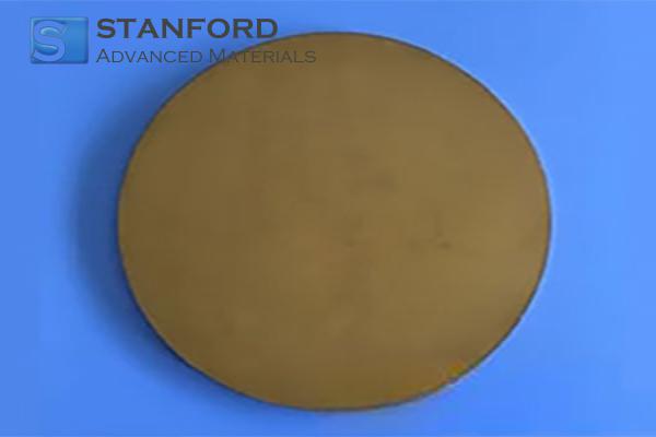
Germanium Selenide (GeSe2) Sputtering Target Description
The Germanium Selenide (GeSe2) Sputtering Target, designated
is a high-purity material engineered for advanced sputtering deposition
processes. Featuring a composition of GeSe₂ and a melting point of 707℃, this
target is optimized for semiconductor and thin-film applications where
precision and performance are crucial. Its customizable shapes, offered as
standard discs or custom-made configurations, ensure compatibility with a
variety of sputtering systems and fabrication requirements.
Germanium Selenide (GeSe2) Sputtering Target Applications
· Semiconductor Manufacturing: Ideal for depositing thin
films in integrated circuits and other semiconductor devices.
· Optoelectronic Devices: Suitable for the creation of infrared optics and
photodetectors.
· Solar Cells: Enhances photovoltaic performance by enabling uniform film
deposition.
· Research and Development: Supports advanced material studies and experimental
thin-film processes.
Germanium Selenide (GeSe2) Sputtering Target Packing
Our Germanium Selenide Sputtering Targets are carefully
packaged to maintain product integrity during storage and transportation.
Custom packaging solutions—such as vacuum-sealed containers—are available to
protect the target from contaminants and ensure optimal performance.
Frequently Asked Questions
Q: What applications are best suited for the Germanium
Selenide (GeSe2) Sputtering Target?
A: It is primarily used in semiconductor manufacturing, optoelectronic devices,
solar cells, and R&D for advanced thin-film deposition processes.
Q: Why is high purity (≥99%) important for this sputtering
target?
A: High purity minimizes contamination during deposition, ensuring superior
film quality and consistent device performance.
Q: Can the target be customized beyond standard disc shapes?
A: Yes, the target is available in custom-made shapes to meet specific
equipment or application requirements.
Q: How does the melting point of 707℃ influence its use?
A: A melting point of 707℃ ensures the target maintains structural integrity
during high-temperature sputtering processes, providing stable and reliable
deposition.
Q: What does "Sputter: N/A" indicate in the
product information?
A: It indicates that no specific sputter method is associated with this target,
meaning it is designed for direct use in sputtering deposition processes
without additional modifications.
 바
바
 비즈 & 구체
 볼트 및 너트
 도가니
도가니
 디스크
디스크
 섬유 및 원단
 영화
영화
 플레이크
플레이크
 폼
폼
 호일
호일
 과립
과립
 벌집
벌집
 잉크
잉크
 라미네이트
라미네이트
 덩어리
덩어리
 메시
메시
 메탈라이즈드 필름
 플레이트
플레이트
 파우더
파우더
 Rod
Rod
 시트
시트
 단결정
단결정
 스퍼터링 타겟
 튜브
튜브
 워셔
워셔
 전선
전선
 변환기 및 계산기
 글쓰기
글쓰기

 Sputtering Target")
 Sputtering Target")

 Sputtering Target")
 Sputtering Target")
 Sputtering Target")
 Sputtering Target")