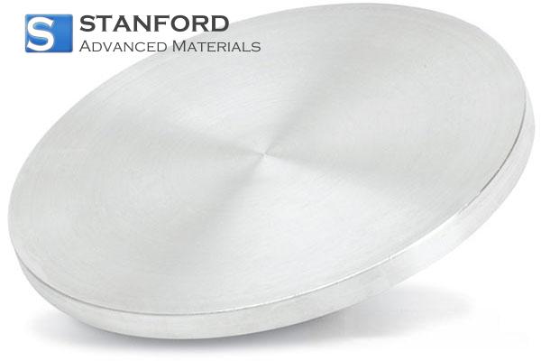
Germanium Silicon (Ge/Si) Sputtering Target Description
The Germanium Silicon (Ge/Si) Sputtering Target is developed
using state-of-the-art fabrication techniques to achieve exceptional uniformity
and purity. Designed specifically for sputtering applications, this target
delivers outstanding performance in thin film deposition processes. Its unique
composition (Ge/Si) ensures reliable operation in demanding semiconductor and
electronic fabrication environments. The material's compatibility with both
indium and elastomer bonding enables it to be adapted for various custom
configurations, making it an ideal choice for both experimental and
high-throughput manufacturing setups.
Germanium Silicon (Ge/Si) Sputtering Target Applications
· Thin Film Deposition: Essential for forming high-quality
layers in semiconductors and optoelectronic devices.
· Semiconductor Manufacturing: Used in the production of integrated circuits
and advanced microelectronic components.
· Photovoltaic Devices: Facilitates the deposition of precise thin films for
efficient solar cell production.
· MEMS Fabrication: Ideal for microelectromechanical systems where material
consistency and precision are critical.
Germanium Silicon (Ge/Si) Sputtering Target Packing
Our sputtering targets are handled with extreme care during
packaging and transportation. Each unit is packaged in a clean-room environment
to ensure it remains free from contaminants and maintains its pristine
condition. Custom packaging options are available to meet the specific needs of
our clients.
Frequently Asked Questions
Q: What are the primary advantages of using a Ge/Si
sputtering target?
A: Ge/Si sputtering targets offer excellent purity and compatibility with
advanced thin film deposition processes, ensuring consistent and high-quality
output for electronic applications.
Q: Can the shapes of the sputtering target be customized?
A: Yes, the targets can be manufactured in standard disc shapes or custom-made
according to your specific application requirements.
Q: What industries typically use Ge/Si sputtering targets?
A: These targets are predominantly used in semiconductor manufacturing,
photovoltaic device production, MEMS fabrication, and advanced electronic
research.
Q: How is the quality and purity of the sputtering target
maintained?
A: Our production process adheres to strict quality control standards, and each
target is produced under controlled conditions to ensure a purity level of
≥99%.
Q: Are there specific storage requirements for Ge/Si
sputtering targets?
A: It is recommended to store the targets in a clean, dry environment with
minimal exposure to contaminants to maintain their integrity until
installation.
 바
바
 비즈 & 구체
 볼트 및 너트
 도가니
도가니
 디스크
디스크
 섬유 및 원단
 영화
영화
 플레이크
플레이크
 폼
폼
 호일
호일
 과립
과립
 벌집
벌집
 잉크
잉크
 라미네이트
라미네이트
 덩어리
덩어리
 메시
메시
 메탈라이즈드 필름
 플레이트
플레이트
 파우더
파우더
 Rod
Rod
 시트
시트
 단결정
단결정
 스퍼터링 타겟
 튜브
튜브
 워셔
워셔
 전선
전선
 변환기 및 계산기
 글쓰기
글쓰기

 Sputtering Target")
 Sputtering Target")

 Sputtering Target")
 Sputtering Target")
 Sputtering Target")
